
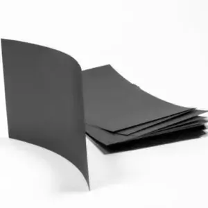
thermally conductive hpms graphite
At NEDC, we like to think we are experts in thermal interface materials. Flexible graphite material is an excellent thermally conductive material. In fact, I see a lot of thermal interface pads going in this direction due to its great thermal conductivity, & low thermal impedance. In this blog, I wanted to mention a thermal pad type that stands above all the rest in the thermal conductivity category: HPMS Graphite
Properties of HPMS Graphite:
Conductivity In-Plane: 1800 W/m-K (think about that number its 5 times that of copper, 5 times!)
Conductivity Through-Plane(Varies): 10- 26 W/m-K
Applications for Flexible Graphite Sheets
Applications for HPMS Graphite include computer servers, gaming systems, telecommunications, peripherals, and various electronics. In these applications, the flexible graphite serves as either a heat spreader, Z heat transfer, or as EMI shielding, absorbing in electronics.
What I like about HPMS Thermally Conductive Graphite:
There’s a number of things I like about this material. I’m going just name my two favorite things below because otherwise I’m just repeating all the features :).
It’s not often that we come across a graphite solution that can withstand consistent flexing. Most graphites when bent, immediately crumble. This can be especially frustrating during converting/die-cutting, or even packaging of this material. In addition, these thermal pads provide the highest level of thermal conductivity in the X-Y direction.
More Information
Thicknesses for this flexible graphite include the thin gauges of.012mm, .017mm, .025mm, .040mm, .050mm, .070mm and .100mm. Naturally, the graphite comes in a silver gray color. NEDC is a die cutter that makes custom die-cut products, shapes and sizes for customers. When converting graphite, conventional die cutting is the only thing that works, laser, nor knife works real well. This graphite is available with an adhesive backing for ease in an assembly. For more information on thermally conductive graphite material, please contact sales@nedc.com.